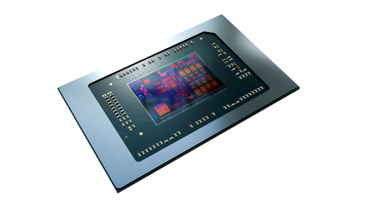
Last month, in a press interview, Jack Huynh, AMD's senior vice president and general manager of the Computing and Graphics Business Unit, confirmed the existence of Kraken Point. This new processor is an 8-core, 16-thread chip that serves as a scaled-down version of the Strix Point. The Kraken Point is anticipated to debut at the major CES 2025 event, slated for early 2025.

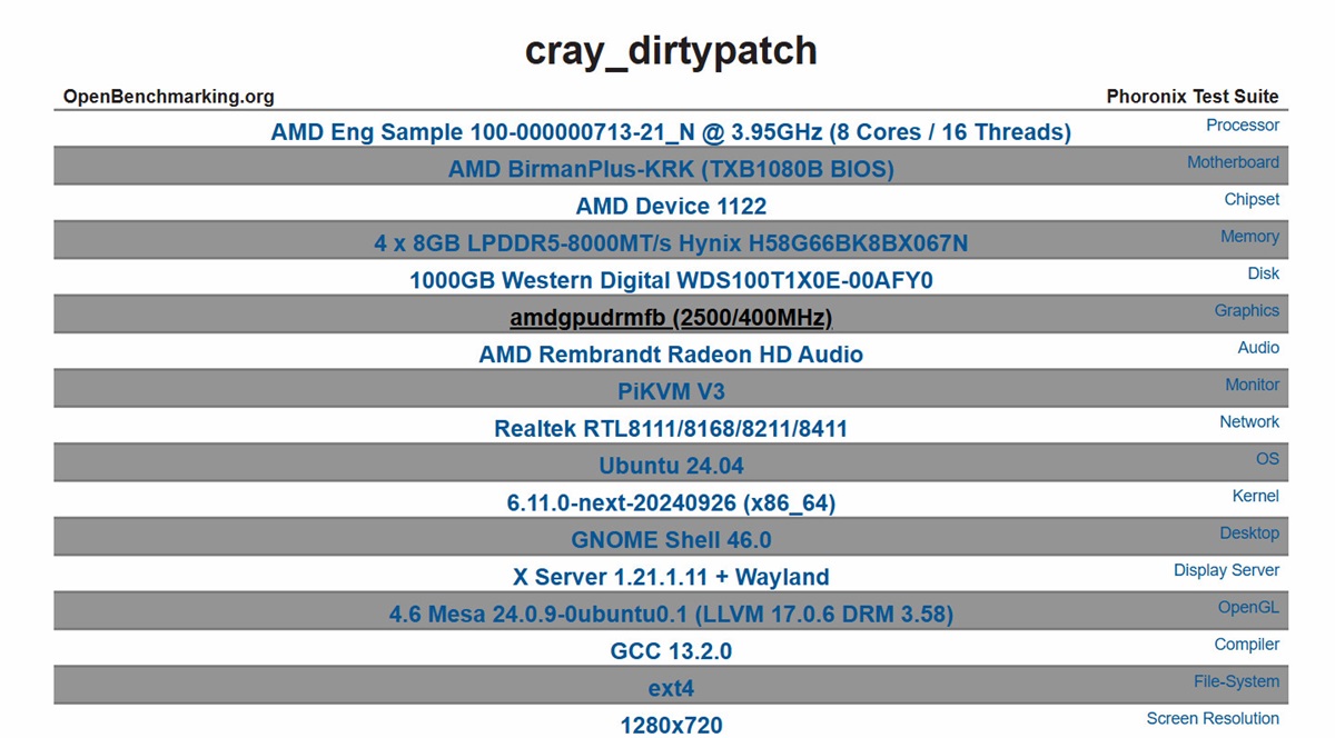
Recently, a keen observer discovered Kraken Point listed in a benchmark database. It was identified with a product ID of 100-000000713 and was tested on an AMD BirmanPlus-KRK motherboard. The processor ran at 3.95GHz, sporting a 1TB Western Digital WD_BLACK SN850 SSD and 32GB of LPDDR5(X)-8000 memory. Given that this is an engineering sample, some specifications, such as the frequency, might differ from the final retail version.
Kraken Point combines four Zen 5 and four Zen 5c cores, featuring a 16MB L3 cache. Its GPU is based on the RDNA 3.5 architecture, including eight compute units (CUs), and it is equipped with an NPU featuring the XDNA 2 architecture. This NPU offers 50 TOPS of AI computational power and is expected to meet Microsoft Copilot+ PC certification standards. Moreover, Kraken Point employs an FP8 platform with a configurable TDP ranging between 15 to 45 watts and is projected to be fabricated using a cutting-edge 4nm process.

While comparing it to Strix Point, Kraken Point features four fewer Zen 5c cores and a reduced number of CUs. Interestingly, the NPU remains unaltered to fulfill the computational demand for Microsoft Copilot+ PCs. The transition to a 4+4 core structure negates the need for dual CCXs, thus eliminating the core communication latency issue found in Strix Point. With its reduced size, the production cost of the chip naturally drops, enabling it to cater to a broader market.