AMD's Next-Gen Zen 6 Architecture APU Core Configuration Exposed
Recently, some foreign media have revealed the core configurations of AMD's upcoming Zen 6 architecture mobile processor series, called Medusa Point. According to the exposed details, the flagship Ryzen 9 model will feature up to 22 cores, promising a substantial enhancement in multi-threaded performance. However, it entails a reduction in GPU configuration, featuring integrated graphics (iGPU) with the RDNA 3.5+ architecture, and the computing units (CUs) will be decreased to 8, indicating a compromise compared to its predecessor.

Medusa Point represents a significant step in AMD's mobile APUs, succeeding the Zen 5 architecture seen in the Strix Point and Strix Halo series, which form the backbone of AMD's mobile product lineup. The Ryzen 5 and Ryzen 7 variants will include a 10-core design composed of four Classic Cores, four Dense Cores, and two Low-Power Cores, paired with eight RDNA 3.5+ compute unit iGPUs. The Ryzen 9 models take it further by incorporating an additional 12-core chip complex (CCD) on top of the 10-core unified chip, creating a total 22-core configuration, though the iGPU remains fixed at 8 compute units. This Multi-Chip Module (MCM) strategy is AMD's first venture into mobile processors delivering desktop-grade, high-core-count capabilities to boost multi-threaded task performance in notebooks.
The Zen 6 architecture is pivotal to the Medusa Point's leap in performance. Unlike previous Zen architectures that maxed out at eight cores per single-chip complex, Zen 6 allows for up to 12 cores per single-chip complex and employs a mix of classic, high-density, and low-power core types. This strategy appears to draw inspiration from Intel's hybrid core approach, aimed at balancing performance with energy efficiency. While some users initially resisted Intel's approach of combining large and small cores, it is evident that such hybrid designs are future-oriented, offering efficiency as software evolves to handle scheduling tasks more effectively.

Focusing on the Zen 6 architecture's Medusa Point, the tri-core design comprises classic cores dedicated to resource-intensive tasks like gaming and video rendering, high-density cores for multithreaded lightweight tasks offering efficient parallel processing, and low-power cores for background tasks and minimal-load scenarios to extend battery life. The 22-core Ryzen 9 variants are exceptionally suited for mobile workstations requiring robust multi-threaded performance, ideal for 3D modeling, virtualization, or scientific computations.
Regarding packaging technology, Medusa Point employs an FP10 package, slightly larger than the FP8 package used in Strix Point, measuring roughly 25mm x 42.5mm—an area increase of about 6%. The increased size can accommodate better thermal designs and component layouts internally, facilitating consistent high-performance in thin and light laptops. Certain Medusa Point models utilize a monolithic chip design with integrated 10 cores and iGPU, where the Ryzen 9 model adds a 12-core chip complex to the primary chip through Interchip Fabric (I/F), alongside a separate I/O chip (IOD) hosting the memory controller, media engine, and interface modules. Such modular architecture not only augments core count but also offers upgrade flexibility.
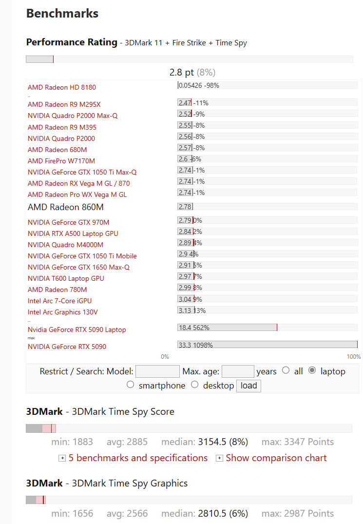
The Medusa Point's iGPU configuration has, unsurprisingly, sparked discussion. While the Strix Point's Radeon 890M contains 16 RDNA 3.5 compute units, Medusa Point reduces its iGPUs to 8 compute units, estimating comparable to Radeon 860M. Performance tests indicate a 20-25% graphics performance reduction compared to the Radeon 890M, potentially impeding the flagship model's smooth prowess in 1080p gaming scenarios. Optimized RDNA 3.5+ enhances energy efficiency and specific workloads, yet lacks RDNA 4 architecture support, missing out on the latest ray tracing and AI acceleration technologies. This suggests AMD targets enhanced CPU performance with Medusa Point, distinguishing it from Strix Halo's successor, which emphasizes high-performance graphics processing.
On the manufacturing front, Medusa Point's Zen 6 cores utilize TSMC's 3nm (N3P) process, while the I/O chips employ the more affordable 4nm (N4P) technology. The 3nm process offers higher transistor density and energy efficiency, maintaining power consumption in check amid high core counts, thus boosting single-thread performance. Contrarily, Strix Halo's Zen 5 cores are produced via a 4nm process, highlighting Medusa Point's advantageous hardware refinement contributing to performance gains. Regarding memory support, Medusa Point is anticipated to be compatible with LPDDR5X memory, potentially reaching 7,500MT/s maximum rate, matched with a 128-bit memory controller to ease bandwidth demands arising from high core counts.
Market-wise, Medusa Point aims at the high-end mobile computing sector, particularly thin and light notebooks or mobile workstations necessitating strong multi-threaded capability. Its 22-core Ryzen 9 model excels in multi-threaded tasks (e.g., video encoding, VM operations), potentially directly competing with Intel's forthcoming Panther Lake series. This new series is projected to leverage an 18A process with an integrated Xe3-architecture iGPU for superior graphics performance, likely trailing Medusa Point's core count.
AMD's strategic direction for Medusa Point appears concentrated on CPU performance-driven mobile processors, exploiting core quantity and architectural benefits to attract professional clientele, leaving premier iGPU performance for the anticipated Medusa Halo series. This next-gen product line achieves unprecedented core counts with its Zen 6 architecture and multi-chip design, infusing desktop-grade multi-threaded processing into mobile platforms. The processor series is expected to be launched in the second quarter of 2026, with CES 2026 possibly serving as its unveiling platform.
أخبار ذات صلة
- TSMC Completes Trial Production of 2nm Process with an Impressive 90% Yield
- Intel Confirms Nova Lake Processors, Adopting 14A Process Technology
- GIGABYTE Launches AI TOP ATOM Desktop Supercomputer Delivering 1000 TOPS Performance
- Intel Official Website Unveils Arc B750 Graphics Card
- AMD to Split MI400 into Two Series Next Year
- Rumor Has It: Intel to Launch Arc B770 Graphics Card Later This Month
- Xe3 Is Not Yet Launched, But Xe4 Is Already on the Horizon: Intel Moves Quickly
- A Sneak Peek at AMD's Zen 6 Architecture, Possibly Debuting with EPYC
- Geekbench Scores Released for NVIDIA's First GB10 Chip Based on Arm Architecture
- Intel and Microsoft Sign Major 18A Foundry Agreement, Sparking Interest from Multiple Companies