TSMC is experiencing unprecedented demand for Artificial Intelligence (AI) chips, and the market demand for NVIDIA's data center GPUs has increased substantially. To meet customer orders, it has been continuously targeting the construction of new facilities. One of the bottlenecks is CoWoS packaging capacity, for which TSMC is actively exploring new packaging technologies in addition to expanding capacity.
According to related media reports, an industry source recently revealed that TSMC is developing a new advanced chip packaging technology that will use rectangular substrates instead of traditional round wafers. This innovation allows more chips to be placed on a single substrate, thus meeting the manufacturing needs of future AI chips. Although the research is still in its early stages and may be several years away from production readiness, it represents a significant technological shift, positioning TSMC once again at the forefront of chip manufacturing technology.
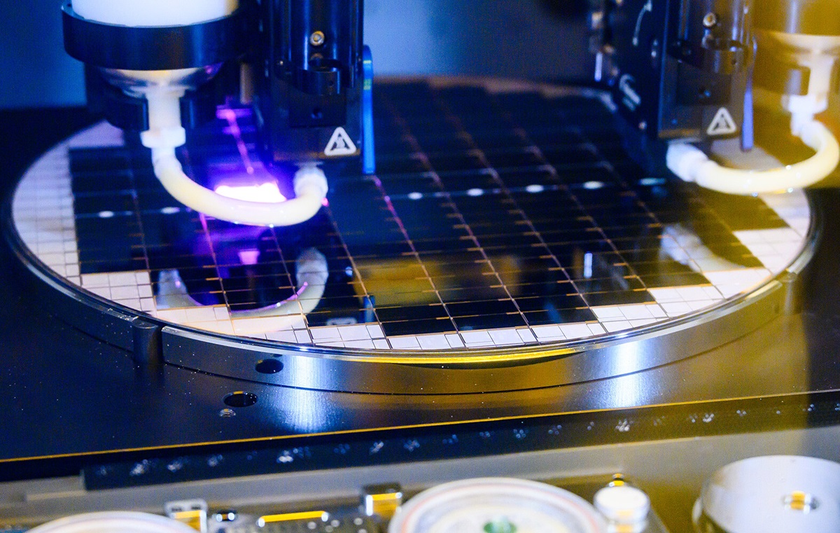
It is understood that TSMC is testing a rectangular substrate size of 515mm x 510mm. Compared to the current 12-inch (300mm) wafers, the available area is more than 3.7 times larger, better meeting the market demand for chips. The use of rectangular substrates can also better eliminate incomplete chips on the edges of round wafers. Although it may seem like only the shape of the wafers has changed, it actually requires a complete revamp of the entire manufacturing process.
TSMC responded to media reports by stating that it is closely monitoring advancements and developments in advanced packaging technologies, including panel-level packaging technology.


